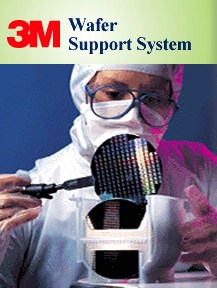
Wafer Inspection Services
Die inspection and wafer inspection services ensure no defects occurred during post-fab processing, such as wafer dicing, backgrinding, and more. Syagrus Systems has a long history of providing superior front-end and back-end wafer and die visual inspection services to the semiconductor industry and other high-precision sectors. We pair fully automated wafer inspection services with the flexibility of manual inspections to ensure no detail is missed and every flaw is identified.
Contact us or request a quote to learn more about our capabilities and semiconductor inspection services.
Front-End and Back-End Die Inspection Capabilities
At Syagrus Systems, our team has the expertise to inspect full wafers as well as sawn wafers on a dicing frame. Our inspection personnel are trained to Mil Std 883 specifications, and we have the capabilities to complete a variety of services:
- Automated wafer inspections to consistently locate defects
- Ability to import wafer maps
- Utilize ink dot recognition
- Image capturing to provide immediate feedback upon request
- Commercial-grade die inspections for products with less stringent requirements
- Wafer and yield data captured automatically by defect class
- Variety of visual die inspection reports upon request, including defect statistics, defect distribution, and more
We are also prepared to work with specific die inspection requirements that fall outside of industry standards. Our wafer inspection services are flexible enough to capture these requirements on our internal travelers and spec sheets, ensuring you receive the level of inspection you require. Call 651-209-6515 for more information.


Die Inspection Identifies Defects and Flaws
Die and wafers must be completely free of defects to be used in semiconductors and other assemblies. Our services are designed to find all defects and flaws, ensuring you receive only the best and most accurate die possible. We identify:
- Metallization, glassivation, and passivation defects
- Polyimide and BCB defects
- Embedded foreign material
- Saw or dicing defects
- Bump defects
- Contamination from liquid residues, surface particles, or adhesive residues
The Benefits of Semiconductor Inspection Services
Semiconductor inspection services raise the output of your production and maximize the efficiency of your final assembly. The benefits of choosing Syagrus Systems for your processing include:
- Higher throughput, resulting in lower manufacturing costs
- Higher quality wafer product
- Improved process control
- Immediate feedback from online data collection and reporting
- Wafer map importing and exporting
- Ink dot recognition capabilities
Choose Syagrus Systems for Reliable Wafer Inspection Services
Syagrus Systems provides world-class front-end and back-end post-fab processing for silicon wafers and semiconductor wafers. All our services are customized to match your standards and meet our strict in-house quality guidelines. Request a quote or contact us to learn more about how we can improve your operations with visual wafer inspection services.Check out other additional wafer services offered by Syagrus: