Wafer Processing & Semiconductor Services for Any Industry
Have a Project Coming Up
Contact Syagrus Today?
Silicon wafers are a key component of semiconductor and integrated circuit manufacturing. As all industries and applications have different specifications, you require an OEM wafer manufacturing partner experienced in silicon wafer processing and semiconductor services for successful product development. Whether you are in the R&D stages or need semiconductors for product manufacturing, you can trust Syagrus Systems to deliver exceptional quality, precision, and customer service.
Contact us to get started.
Commitment to Quality on Every Wafer Processing & Semiconductor Service
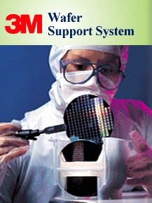
Your complete satisfaction comes through high-quality services that provide high-performance operations. As an ISO 9001:2015 certified and ITAR-registered facility, Syagrus Systems proudly services all segments of the semiconductor industry. We are prepared to tackle the challenges of varied OEM wafer manufacturing orders through our precision wafer processing and semiconductor services:
- Die Pick-and-Place Equipment Manufacturing
- Silicon Wafer Bonding
- Wafer Backgrinding
- Silicon Wafer Dicing
- Wafer Polishing
- Die Sort Services
- And additional wafer processing capabilities!
All dies produced by our wafer processing and semiconductor services undergo rigorous visual inspections to ensure complete compliance with our in-house quality standards, your guidelines, and other necessary regulations. Call 651-209-6515 to speak with an expert representative to learn more about our services, capabilities, and complete commitment to quality wafer processing.
Industries Served
Semiconductor Wafer Manufacturing for OEMs
Available in many shapes and configurations, semiconductors form the building blocks of diodes, transistors, integrated circuits, and much more. To meet the diverse needs of semiconductor manufacturers, we provide a variety of customizable services to match OEM's unique specifications.
Military & Aerospace
Many leading military contractors in the United States choose Syagrus Systems for post-fab wafer processing. Specialty services include MEMS device wafer thinning, ultrathin wafer dicing for RF chips, and stress-free wafer processing for:
- Wearable electronics for pilots and soldiers
- Weapons and surveillance systems
- Airplane controls and sensors
- Drones and other UAVs
- And other sophisticated applications.
Medical Electronic Products
All wafer processing and semiconductor services are performed in our Class 10K cleanroom and rigorously inspected to maintain the specifications required by medical device OEMs. To satisfy the needs of any production, we offer post-fabrication processing capabilities.
RFID Communications
Syagrus Systems specializes in ultrathin wafer processing for RFID communications. Using precision wafer processing and semiconductor services, we reliably produce silicon wafers for RFID components used in an ever-expanding range of applications:
- Supply chain and inventory management
- Materials management
- Tool and personnel tracking
- And many other systems.
Telecommunications & Commercial Electronics
RAM chips are used widely in electronics, computing, and telecommunications. To function properly, these integrated circuits require precision silicon wafers manufactured by a trusted source. Using cutting-edge fabrication techniques and automated processes, we have the capabilities to produce wafers for:
- Smartphones
- Automobile electronics
- Home appliances
- And any other product using electronic circuitry.
Wafer Processing & Research Assistance for Scientific Universities
Many of America’s leading research and scientific universities rely on Syagrus Systems for precision silicon wafer processing and semiconductor services, expert knowledge, and more. In addition to our high-quality manufacturing services, we welcome all students and faculty to ask us about silicon wafer processing for your research projects. We can meet the needs of most projects and have worked with individuals representing:
- MIT
- Georgia Tech
- USC
- UCLA
- Virginia Tech
- Auburn
- The University of Illinois
- UC Santa Barbara
- UC Berkeley
- Notre Dame
- Perdue
- Duke
- And many others.
Choose Syagrus Systems for Precision Wafer Processing & Semiconductor Services
Syagrus Systems is prepared to meet the needs of all industries. Request a wafer processing quote or contact us today to discuss your requirements.