Silicon Wafer Services


Silicon wafers are thin slices of semiconductor material used to fabricate integrated circuits, microdevices, and more. The manufacturing process for silicon wafers involves multiple highly precise stages to achieve the desired thickness, surface finish, and other specifications. Syagrus Systems is one of the industry’s leading post-fab, back-end silicon wafer service providers. Whether you require one or several processes, we have the equipment and expertise to complete your project through fast lead times and worry-free silicon wafer services.
Contact us today to discuss details specific to your project.
Wafer Preparation: Front-End-of-Line Processing
Before back-end wafer services can occur, silicon wafers must undergo front-end-of-line processing (FEOL). FEOL silicon wafer processing involves the formation of transistors directly in silicon. Individual devices, including transistors, capacitors, resistors, and more, are patterned into the semiconductor by interconnecting the isolated transistors to produce the desired electrical circuit.
Syagrus Systems then steps in to provide consistently flexible back-end silicon wafer services to match your specifications and deliver precision results.
Back-End-of-Line Silicon Wafer Processing
Syagrus Systems is a trusted provider of back-end-of-line (BEOL) silicon wafer processes where individual devices are interconnected with the metallization wiring layer of the wafer. Steps, timeline, and price will vary depending on your selected service, production volume, and other factors.
Read below to learn more about our leading silicon wafer services. If you require assistance selecting the best silicon wafer processes for your application, are completing a research project, or have other questions, contact us to speak with a representative directly.
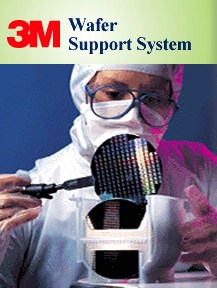
Temporary Silicon Wafer Bonding with 3M™ Wafer Support System
The 3M™ Wafer Support System is an innovative silicon wafer process that temporarily supports wafers during thinning and post-thinning operations. A UV-curable adhesive temporarily bonds wafers to glass, providing additional support and structure with ultra-thin results.
Silicon Wafer Backgrinding

Our wafer thinning and backgrinding processes, or “backlap” processes, create wafers to achieve precision specifications, including:
- Target thicknesses of less than 0.050mm (0.002”)
- Thickness variance under 5 microns
- Thin wafers from 4” to 8” diameter
Wafer Polishing Services
Syagrus Systems’ silicon wafer polishing services utilize Chemical Mechanical Planarization (CMP) to remove between 5-10 microns of silicon from wafer backsides. Wafer polishing:
- Removes stresses
- Prevents warping
- Enhances semiconductor wafers
Wafer Dicing Services

High-precision wafer dicing uses double-pass cutting processes to cut semiconductor wafers into small chips and die. Wafer dicing processes are performed in a Class 10K cleanroom and achieve:
- Extreme accuracy for bumped and non-bumped wafers
- High-volume or low-volume production runs
- Precision cuts as small as 0.006” (0.2mm) and wafers as thin as 0.0008” (0.02mm)
Silicon Wafer and Die Visual Inspection Process
We offer fully automated and manual silicon wafer inspection services for full wafers and sawn wafers on dicing frames. Our wafer and die inspection services:
- Locate defections or damages
- Utilize ink dot recognition
- Provide immediate feedback
- Prevent circulation of faulty wafers
Die-Sorting Services & Processing Equipment Manufacturing
Silicon die-sorting services include fully automated, manual, and multi-die binning processes. Our advanced silicon wafer die-sorting process can work with die less than 50μm in thickness, wafer diameters from 3” to 12”, and much more. Wafer and die sorting services:
- Eliminate defective wafers
- Sort approved wafers and dies
- Maximize yield
- Minimize waste
Additional Silicon Wafer Processing & Capabilities
Syagrus Systems offers additional silicon wafer services to match your application’s needs, including:
- Post-metallization annealing
- Backside metal deposition, sputtering, and evaporation
- Secondary thinning services
Quality Post-Fab Silicon Wafer Services & Manufacturing for Any Industry
Fabless semiconductor manufacturers, large corporations, laboratories, and other manufacturing facilities don’t always have the capability or machinery to accommodate high-volume silicon wafer production. Syagrus Systems provides complete silicon wafer services for these facilities across a range of sectors, including:
- Aerospace & Military
- Commercial electronics
- Medical
- OEMs
- Scientific Universities
- Telecommunications
- And many others!
We have strict quality assurance standards for all processes to ensure control and accuracy, carrying out each service in a safe and clean processing environment. With extensive experience and state-of-the-art silicon wafer processing equipment, we deliver superior results.
Contact Syagrus Systems to Discuss Your Silicon Wafer Processing Needs
Contact us to discuss our post-fab back-end silicon wafer services. Request a quote to begin your process. An expert representative will be in touch as soon as possible.