Silicon Wafer Chemical Mechanical Polishing Services
Silicon wafer polishing services, also called Chemical Mechanical Polishing (CMP) or silicon lapping services, remove between 5 and 10 microns of silicon from the backside of a wafer to dramatically reduce the peaks and valley microdamage left behind by other silicon wafer processes. Designed to deliver an improved wafer for semiconductor fabrication, CMP eliminates stresses and prevents warping for maximized results.
Syagrus Systems provides CMP processes that produce silicon semiconductor wafers to meet or exceed your standards, such as accommodating specific surface roughness requirements. While keeping the wafer damage-free is challenging, our team has the expertise to conduct CMP processes that remove unwanted surface roughness without harming your semiconductor wafers. Contact us or request a quote to get started.
CMP for High Yields
Syagrus Systems specializes in wafer polishing and post-backgrind relief. Our silicon CMP process prepares your wafers for additional services and is ideal for electronic applications requiring flexible circuits. Our in-house capabilities allow us to polish and etch ultra-thin silicon wafers without causing stress or damage to achieve higher yields. Wafer polishing services include:
- Free-standing silicon wafer, fused silica wafer, and glass wafer polishing
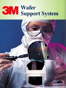
- Bonded wafer stack polishing using the 3M™ Wafer Stack Support System
Safe and Effective Post-Backgrind Silicon Polishing Process
Semiconductor wafer polishing is highly effective and safe for removing stresses and surface damage. Our CMP process uses polishing pads and diamond liquid slurry to polish the wafer. A vacuum carrier holds the wafer in place while leaving the backside exposed. The carrier and wafer are slowly brought into contact with a rotating plate covered with a polishing pad. With a controlled downward force, we carefully remove damaged wafer layers.
Call 651-209-6515 to speak with a representative directly and discuss your order.

How Silicon Wafer Lapping Services Benefit Any Industry
Electronic devices across industries get smaller and thinner with each new generation, which means ultra-thin wafers are in more demand than ever. Our silicon CMP processes are ideal for any project requiring flexible circuits, including:
- OEM Assemblies and Components
- Medical Electronics
- Military & Aerospace Applications
- Semiconductor Fabrication
- And many other precision industries
By incorporating a CMP process into your production, you can ensure a stronger result that operates as designed, produces boosted throughput, lessens the level of surface contamination, and eliminates any residual slurry.
Contact Syagrus Systems to Begin Your Silicon Lapping Services
Syagrus Systems is an ISO 9001:2015-certified provider of full-service solutions for wafers used in semiconductor fabrication and other applications. We follow strict quality control protocols on every order, completing your services in a 10K cleanroom to eliminate the risk of contamination. Our top goal is your complete satisfaction, and we provide quick cycle times to help transition from engineering projects to full production ramp-up. In addition to silicon wafer polishing services, we offer:
Contact us to learn more about our specialized services, and request a quote to receive details specific to your order.