Precision Silicon Wafer Dicing Services


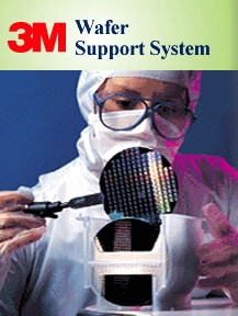
Also called wafer sawing, wafer cutting, and die singulation, wafer dicing is a precision process where semiconductor wafers are cut into small square or rectangular “chips” or “die” that are critical for the quality of all remaining post-fab processes and end-use performances.
We have the expertise, capabilities, and equipment to deliver precision die singulation and wafer dicing services. No job is too big or too small. Request a quote to get started, call 651-209-6515 today to speak directly with a highly trained and knowledgeable representative.
In-House Silicon/Semiconductor Wafer Dicing & Die Singulation Services
At Syagrus Systems, we provide high-quality, ISO 9001:2015 certified silicon wafer dicing standards. Our fully automated silicon wafer dicing capabilities are designed to meet and exceed your specifications by utilizing double-pass cutting to yield superior dies with improved accuracy compared to our competitors. Additionally, all dies are subject to magnification die visual inspection to ensure your wafer performs at peak optimization.
Why Choose Syagrus Systems for Your Wafer Dicing & Die Singulation Service Needs?
Syagrus Systems provides precision silicon wafer dicing and die singulation services to meet your application needs. Advantages include:
- Precision & Low-K Dielectric Expertise – Specialized in low-k dielectric wafers, reducing damage and improving yield.
- Advanced Dicing Technologies – High-precision mechanical blade dicing tailored to your wafer and die requirements.
- Minimal Chipping & Damage Control – Optimized processes ensure high-yield results.
- Die Size & Thickness Flexibility – Handling ultra-thin wafers and custom die sizes.
- Process Customization – Tailored dicing solutions for each client’s needs.
- Post-Dicing Services – Wafer thinning, die sorting, and pick-and-place for a seamless supply chain.
- Industry Focus – Trusted by automotive, medical, and consumer electronics sectors.
- ISO Class Certifications - An ISO 9001:2015 certified (cleanrooms meet or exceed ISO class 7 requirements) and ITAR registered business
Syagrus’ Silicon Wafer Dicing Capabilities
All wafer dicing is performed in a Class 10K cleanroom environment. Same-day cycle time available upon request for fast turnaround on wafer dicing operations. Specific wafer dicing features include, but are not limited to:
- 0.25” (6.35mm) to 12” (300mm) flexible wafer dicing workspace capable of sawing multi-die reticles
- High-precision wafer dicing for singulated devices as small as 0.006” (0.2mm) and wafers as thin as 0.0008” (0.02mm)
- Bumped and non-bumped silicon wafer dicing
- Surfactant available
DFD6362 State-Of-The-Art Wafer Dicer
Syagrus Systems utilizes cutting-edge wafer dicer and surface grinders, providing the best wafer processing solutions available. Syagrus’ new DFD6362 wafer dicer increases throughput by 7%, boosts X-axis and dual cut speed, and improves cleaning and operational efficiency.
Improve Production with Precision Die Singulation Services
Wafer dicing is measured by the yield and quality of the final dies. Effective wafer dicing can improve production output by providing final dies with enhanced quality. We utilize advanced equipment to mount wafers on dicing tape, securing them to a metal frame. Our skilled engineers then cut the wafer with our in-house, high-speed saw to create singular dies. Dies are then inspected and removed safely from the frame via pick and place to prevent unnecessary damage or die flaws.
High and Low-Volume Die Cutting Orders
Syagrus Systems facilitates high-volume and low-volume die cutting orders. Our multi-die cutting system allows us to create multiple quality dies at once. This will enable us to provide quick turnaround times on the dies you need. We can also perform dicing operations on previously singular multi-die reticles and partial wafers.
Additional Post-Fab/Back End Wafer Processing Services
Syagrus Systems is equipped to offer full-service solutions. In addition to die singulation, and depending on your production and goals, we may recommend:
- Wafer Backgrinding reduces wafer thickness to produce ultra-thin wafers for stacking and high-density packaging in compact electronic devices.
- Wafer Polishing removes between 5 and 10 microns of silicon from the backside of a wafer to dramatically reduce the peaks and valley microdamage left behind by other silicon wafer processes.
- Or a variety of other wafer services including Die Visual Inspection, Die Sorting, Backside Metal & Sputtering Deposition & More.
Considerations for Choosing Wafer Sawing Processes
Material hardness/brittleness, thermal sensitivity, desired chip size/geometry, accuracy requirements, and production costs are just a few considerations to be made prior to choosing a wafer dicing process to meet your application needs. Each of our high-precision processes is customizable to match your unique needs.
Wafer Dicing for Semiconductors & Additional Industries
Industrial production lines—including leading semiconductor, military, and medical device manufacturers—require a trusted partner to deliver defect-free die for automated assembly operations. While our precision silicon wafer dicing services are most often utilized by semiconductor and integrated circuit manufacturers, our products and services are prepared to meet the needs of most industries:
- Military and Aerospace
- Medical Electronics
- OEMs
- RFID Communications
- Telecommunications and Commercial Electronics
- Scientific Universities and Research Laboratories
Contact Syagrus Systems for Precision Silicon Wafer Dicing & Processing
Syagrus Systems provides world-class post-fab processing for silicon wafers and semiconductor wafers. As an ISO 9001:2015 certified wafer dicing manufacturer, we are dedicated to continuously improving our services to give you a competitive edge.
Contact us at (651) 209-6515 to speak with an expert, or request a quote to begin your wafer cutting order today.