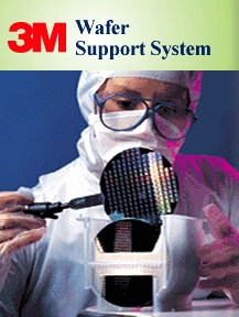
Wafer Bonding Services with the 3M™ Wafer Support System
Semiconductor manufacturers and other users often need ultrathin silicon wafers. However, the thinner wafers get, the more fragile they become. A highly effective solution is using temporary wafer bonding to minimize stress on silicon wafers during processing. Other benefits to wafer bonding services include protecting wafers from damage during conventional thinning and post-thinning processes, non-damaging adhesives that are easily peeled away, and higher yields.
Syagrus Systems is your full partner for any wafer processing service. We ensure a production with higher yields, high throughput, and reduced waste. Our team is highly experienced in wafer bonding. We use top-of-the-line programmable technology and proven methods, such as the 3M™ Wafer Support System, to consistently achieve wafer thicknesses of 50μm or less. Thinner or thicker wafers can be created by special request.
How the 3M Wafer Support System Benefits Your Wafer Bonding Service
Syagrus Systems utilizes the 3M Wafer Support System, a proven method of manufacturing ultrathin wafers. This reliable and efficient system combines 3M bonding chemistries with state-of-the-art equipment and was explicitly designed for semiconductor manufacturing. It is compatible with high-temperature and high-vacuum processes, typical process chemistries, and low-k dielectric materials.
The key component of the 3M Wafer Support System is a special UV-curable adhesive formulated specifically for temporary wafer bonding to glass. The 3M adhesive is spun onto the wafer surface and bonded under vacuum to ensure no air bubbles or other voids are trapped between the wafer and the support glass. The adhesive flows into and supports the topography of the circuit patterns on the front side of the wafer, enhancing your bonding process to provide many advantages compared to using tape:
- More uniform, rigid support surface
- Minimized stress on the wafer
- Wafer thinning to less than 20µm final thickness
Temporary Wafer Bonding for 3M Wafer Support Systems | Syagrus Systems from Syagrus Systems on Vimeo.
Precision Wafer Bonding Processes
Syagrus Systems has been providing precision silicon wafer bonding services for many years. Call 651-683-2220 to learn more about how our services can support your manufacturing goals.
How the Silicon Wafer Bonding Process Works


Glass Substrate Support Protects Silicon Wafers During Processing
After wafer bonding and processing, the glass substrate continues to provide support for post-grinding processes such as etch, CMP, or metal deposition. After services are completed, a special laser is used to debond the glass carrier plate, allowing for easy, chemical-free separation using minimal force. No heat, wet chemistry, or soaking is required to separate the silicon wafer from the glass substrate. Because the temporary wafer bonding process supports the entire face and edges of the wafer, it results in less warpage, cracking, and edge chipping.
Light to Heat Conversion Coating Services for Silicon Wafers
The Light to Heat Conversion (LTHC) layer is applied via spin coating and cured for use with the 3M Wafer Support System wafer bonding process. We verify all glass substrates after coating for proper levels of light transmittal.
High Yields & Quality Results for Any Industrial Project
Syagrus Systems provides highly efficient and effective wafer bonding services that deliver exceptional results. We are proud to produce wafers that enhance operations across industries:
- Semiconductor manufacturing
- Medical electronic products
- RFID communications
- Telecommunications & commercial electronics
- And many other applications!
Choose Syagrus Systems for Your Wafer Bonding & Other Processing Services
Syagrus Systems is one of the most trusted names in the semiconductor wafer processing industry. In addition to wafer bonding, we offer a variety of other silicon wafer processing services:
Our services are designed to produce high-yield silicon wafers that match your specifications. We adhere to strict quality standards to ensure that you receive only the best final products for your application. Your success is our success, and we aim to deliver your complete satisfaction through flexible services, fast turnarounds, and high-quality outputs.
Request a quote on temporary wafer bonding or contact us to discuss your wafer processing needs.